
In electronics manufacturing, printed circuit boards (PCBs) are the backbone of countless devices, from smartphones and laptops to medical equipment and automotive systems. Understanding the intricacies of PCB board layers. It is essential for engineers, designers, and manufacturers alike. At Vision Technology. We’re dedicated to demystifying the complexities of PCBs and providing you with the knowledge you need to succeed. This comprehensive guide will explore everything you need about PCB board layers, from their composition and construction to common issues and best practices. Let’s dive in and unravel the mysteries of PCB board layers together.
Understanding PCB Board Layers
What Are PCB Board Layers?
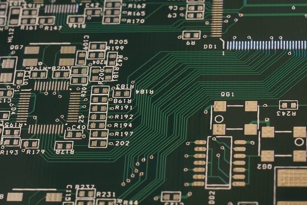
A printed circuit board (PCB) is a flat board made of non-conductive material, typically fiberglass, that serves as a base for mounting electronic components. PCBs consist of one or more conductive layers, known as copper traces, which provide pathways for electrical signals to flow between components.
The Composition of PCB Board Layers
PCBs are constructed using a layering process, where multiple layers of conductive and non-conductive materials are bonded together to create a single integrated circuit board. The number of layers in a PCB can vary depending on the design’s complexity and the application’s requirements.
Common Types of PCB Board Layers
- Single-Layer PCBs: Also known as single-sided PCBs, these boards consist of a single layer of conductive material (usually copper) on one side of the substrate.
- Double-Layer PCBs: Double-layer PCBs feature conductive material on both sides of the substrate, allowing for more complex circuit designs and higher component density. They are widely used in consumer electronics, automotive systems, and industrial applications.
- Multi-Layer PCBs: Multi-layer PCBs contain three or more layers of conductive material sandwiched between insulating substrate layers. Multi-layer PCBs offer greater flexibility, higher component density, and improved signal integrity, making them ideal for high-performance applications.
Surface Mount PCB Board: A Closer Look
Surface-mount technology (SMT) is a popular method for assembling PCBs. In this method, components are mounted directly onto the board’s surface. Surface-mount PCB boards offer several advantages over traditional through-hole assembly, including smaller sizes, higher component densities, and faster assembly times.
Common Issues with PCB Board Layers
- PCB Damage: PCBs are susceptible to damage from various sources, including physical stress, moisture, heat, and electrical overload. Common types of PCB damage include delamination, solder joint fractures, and component failures.
- Signal Integrity Issues: Signal integrity is critical in high-speed digital and analog circuits. Common signal integrity issues include noise, crosstalk, and impedance mismatches, which can degrade performance and reliability.
- Thermal Management Challenges: Heat dissipation is a significant concern in PCB design, particularly in applications with high power densities or operating temperatures. Inadequate thermal management can lead to component overheating, reliability issues, and premature failure.
Flex PCB Manufacturer: Innovations in PCB Design
Flexible printed circuit boards (PCBs) offer unique advantages over traditional rigid PCBs, including flexibility, lightweight, and space-saving capabilities. They are commonly used in applications where space constraints, mechanical flexibility, or dynamic movement are critical factors.
Best Practices for Designing PCB Board Layers
- Plan: Start by clearly understanding your project requirements, including size constraints, component placement, and signal integrity considerations.
- Use Proper Layer Stackup: Proper layer stackup is critical for achieving optimal signal integrity, thermal management, and manufacturability. Consider signal routing.
- Minimize Signal Crosstalk: Signal crosstalk occurs when signals from adjacent traces interfere, leading to signal degradation and performance issues. To minimize signal crosstalk, maintain adequate spacing between traces and use proper signal routing techniques.
- Optimize Grounding: Proper grounding is essential for minimizing noise, reducing electromagnetic interference (EMI), and improving signal integrity. Use dedicated ground planes and ensure a low-impedance path for return currents.
- Consider Environmental Factors: Consider the environmental conditions in which your PCB will operate, including temperature, humidity, vibration, and shock. Choose materials and design features that can withstand these conditions without compromising performance or reliability.
Choosing the Right Turnkey Supplier
At Viasion Technology, we’re committed to delivering high-quality PCB solutions tailored to your specific needs. From quick-turn circuit boards to PCB layout services and turnkey PCB assembly, we offer comprehensive turnkey solutions to help you bring your project to life. Contact us today to learn more about our services and how we can support your PCB manufacturing needs.
Read more: Demystifying PCB Board Layers: Everything You Need to Know.